
Dispositif à pression assemblée de contrôle de thyristor
Obtenir le dernier prix| Type de paiement: | L/C,T/T,Paypal |
| Incoterm: | FOB,CFR,CIF |
| transport: | Ocean,Air |
| Hafen: | SHANGHAI |

| Type de paiement: | L/C,T/T,Paypal |
| Incoterm: | FOB,CFR,CIF |
| transport: | Ocean,Air |
| Hafen: | SHANGHAI |
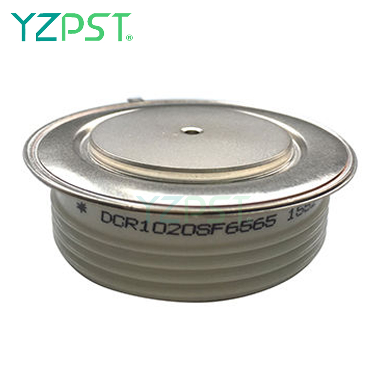
Modèle: YZPST-DCR1020SF65-1
marque: YZPST
| Type de colis | : | 1. Emballage anti-électrostatique 2. Boîte en carton 3. Emballage de protection en plastique |
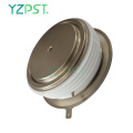
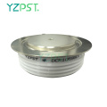
Thyristor haute puissance
YZPST-DCR1020SF65-1
application de thyristors thyristors à moteur à courant continu à thyristors Toutes les valeurs nominales sont spécifiées pour Tj = 25 oC, sauf indication contraire.
(1) Toutes les tensions nominales sont spécifiées pour une forme d'onde sinusoïdale appliquée de 50 Hz / 60 Hz sur la plage de températures comprise entre -40 et +125 oC.
(2) 10 ms. max. largeur d'impulsion
(3) Valeur maximale pour Tj = 125 oC.
(4) Valeur minimale pour la forme d' onde linéaire et exponentielle jusqu'à 80% du VDRM nominal. Porte ouverte. Tj = 125 oC.
(5) Valeur non répétitive.
(6) La valeur de di / dt est établie conformément à la norme EIA / NIMA RS-397, chapitre 5-2-2-6. La valeur définie serait en outre
celle obtenue à partir d'un circuit amortisseur, comprenant un condensateur de 0,2 F et une résistance de 20 ohms en parallèle avec le thristor sous test.
Caractéristiques:. Toutes les structures diffuses . Configuration de porte d’amplification centrale . Capacité de blocage jusqu'à 4200 volts
. Temps d'arrêt maximum garanti . Capacité élevée de dV / dt . Dispositif assemblé sous pression

|
Parameter |
Symbol |
Min. |
Max. |
Typ. |
Units |
Conditions |
|
Average value of on-state current |
IT(AV) |
|
640 |
|
A |
Sinewave,180o conduction,T =60oC c |
|
RMS value of on-state current |
ITRMS |
|
1005 |
|
A |
Nominal value |
|
Peak one cPSTCle surge (non repetitive) current |
ITSM |
|
-
8.5 |
|
KA KA |
8.3 msec (60Hz), sinusoidal wave- shape, 180o conduction, T = 125 j oC 10.0 msec (50Hz), sinusoidal wave- shape, 180o conduction, T = 125 j oC |
|
I square t |
I2t |
|
0.36x10⁶ |
|
A2s |
8.3 msec and 10.0 msec |
|
Latching current |
IL |
|
600 |
|
mA |
VD = 24 V; RL= 12 ohms |
|
Holding current |
IH |
|
200 |
|
mA |
VD = 24 V; I = 2.5 A |
|
Peak on-state voltage |
VTM |
|
3.6 |
|
V |
ITM = 1800 A; Duty cPSTCle 0.01%; T = 25 oC j |
|
Critical rate of rise of on-state current (5, 6) |
di/dt |
|
- |
|
A/ s |
Switching from VDRM 1000 V, non-repetitive |
|
Critical rate of rise of on-state current (6) |
di/dt |
|
100 |
|
A/ s |
Switching from VDRM 1000 V |
E L E CTR I C A L CH A R A T E R IS T I C S A N D R A T I N G S
|
G a t i n g
|
Parameter |
Symbol |
Min. |
Max. |
Typ. |
Units |
Conditions |
|
Peak gate power dissipation |
PGM |
|
150 |
|
W |
tp = 40 us |
|
Average gate power dissipation |
PG(AV) |
|
5 |
|
W |
|
|
Peak gate current |
IGM |
|
- |
|
A |
|
|
Gate current required to trigger all units |
IGT |
|
- 300 - |
|
mA mA mA |
V = 6 V;R = 3 ohms;T = -40 oC D L j V = 6 V;R = 3 ohms;T = +25 oC D L j V = 6 V;R = 3 ohms;T = +125oC D L j |
|
Gate voltage required to trigger all units |
V |
|
- 3.0 - |
|
V V V |
V = 6 V;R = 3 ohms;T = -40 oC D L j V = 6 V;R = 3 ohms;T = 0-125oC D L j VD = Rated VDRM; RL = 1000 ohms; T = + 125 oC j |
|
Peak negative voltage |
VGRM |
|
5 |
|
V |
|
D y n a m i c
|
Parameter |
Symbol |
Min. |
Max. |
Typ. |
Units |
Conditions |
|
Delay time |
td |
|
- |
0.5 |
s |
ITM = 50 A; VD = Rated VDRM Gate pulse: VG = 20 V; RG = 20 ohms; tr = 0.1 s; tp = 20 s |
|
Turn-off time (with VR = -50 V) |
tq |
|
- |
600 |
s |
ITM = 1000 A; di/dt = 25 A/ s; VR -50 V; Re-applied dV/dt = 20 V/ s linear to 80% VDRM; VG = 0; T = 125 oC; Duty cPSTCle j 0.01% |
|
Reverse recovery charge |
Qrr |
|
* |
|
C |
ITM = 1000 A; di/dt = 25 A/ s; VR -50 V |
* O r F gu a r a n t eed m a x . v a lu e , c on t a c t f a c t o r y
T H E R M A L A N D ME CH A N I C A L CH A R A T E R IS T I C S A N D R A T I N G S
|
Parameter |
Symbol |
Min. |
Max. |
Typ. |
Units |
Conditions |
|
Operating temperature |
Tj |
-40 |
+125 |
|
oC |
|
|
Storage temperature |
Tstg |
-40 |
+125 |
|
oC |
|
|
Thermal resistance - junction to case |
R (j-c) |
|
0.022 0.052 |
|
o C/W |
Double sided cooled Single sided cooled |
|
Thermal resistamce - case to sink |
R (c-s) |
|
0.004 0.008 |
|
o C/W |
Double sided cooled * Single sided cooled * |
|
Thermal resistamce - junction to sink |
R (j-s) |
|
- - |
|
o C/W |
Double sided cooled * Single sided cooled * |
|
Mounting force |
P |
18 |
22 |
|
kN |
|
|
Weight |
W |
|
|
- |
g |
|
* M o n t i ng s ur f a c es s m oo t h, f l a t et g r e a é s
PLAN DE CAS ET DIMENSIONS


Numéro De Téléphone: 86-514-87782298
Whatsapp: +8613805278321
Adresse De Compagnie: 3rd Floor, Weiheng Building No.20 B Area, Yangzhou, Jiangsu China
site Web: https://fr.yzpst.com


Privacy statement: Your privacy is very important to Us. Our company promises not to disclose your personal information to any external company with out your explicit permission.
Fill in more information so that we can get in touch with you faster
Privacy statement: Your privacy is very important to Us. Our company promises not to disclose your personal information to any external company with out your explicit permission.